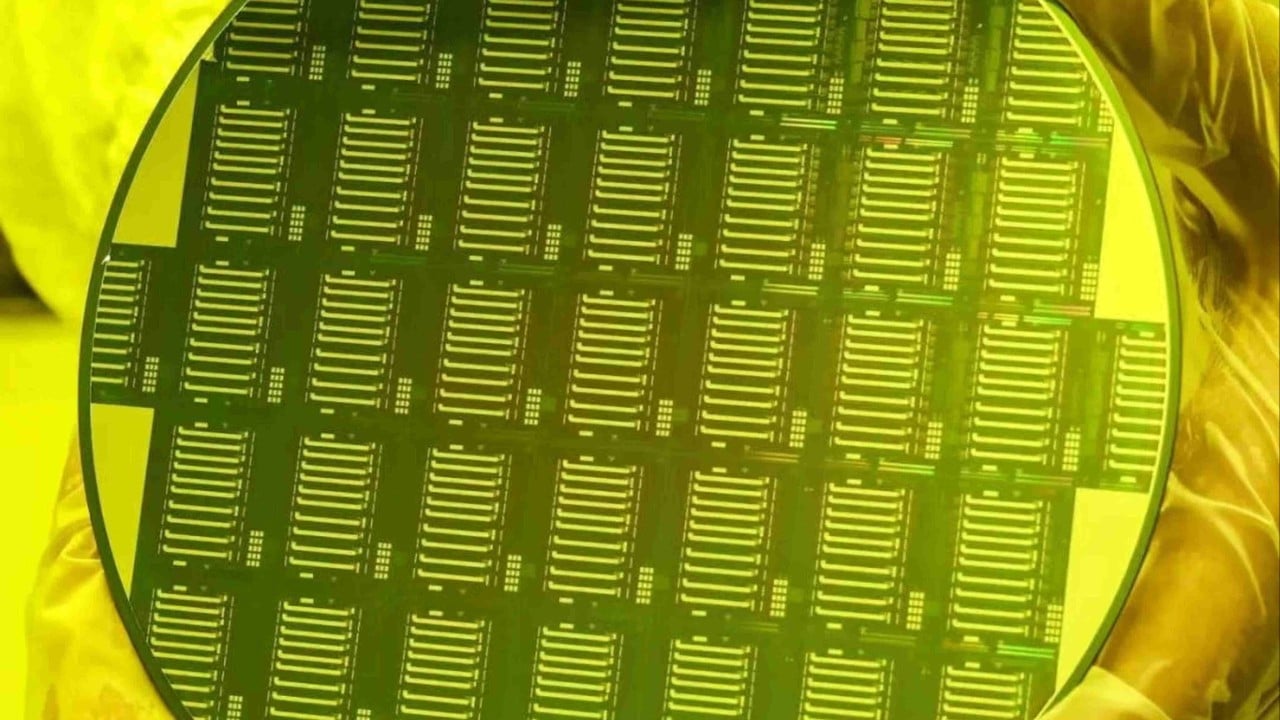
United States export controls targeting China’s semiconductor ecosystem operate on a fundamental premise: weaponizing mechanical bottlenecks in advanced extreme ultraviolet (EUV) lithography stops a nation from scaling artificial intelligence compute. By restricting entities like SMIC from acquiring ASML’s high-numerical aperture systems, Western sanctions artificially cap Chinese silicon fabrication at the $7\text{ nm}$ or $5\text{ nm}$ threshold using highly inefficient deep ultraviolet (DUV) multi-patterning.
This policy assumes that computing power must scale along the traditional trajectory of electronic microelectronics, defined by packing more microscopic transistors onto a two-dimensional silicon die.
Silicon photonics fundamentally disrupts this assumption by shifting the primary medium of information transfer from electrons to photons. Instead of forcing electrons through increasingly narrow, high-resistance copper interconnects on a traditional chip, optical computing routes light through microscopic silicon waveguides.
Because photons do not possess mass or charge, they do not experience Joule heating (resistive power loss) or parasitic capacitance. The critical strategic implication is clear: optical computing allows a nation to scale computing performance through spatial parallelization and speed-of-light propagation, rendering the structural lack of sub-$3\text{ nm}$ EUV lithography far less relevant.
China’s recent launch of a specialized national photonics laboratory represents a calculated pivot from a losing game of electronic catch-up to a structural leapfrog strategy. This analysis deconstructs the architecture, mechanics, and friction points of this geopolitical technology shift.
The Three Bottlenecks of Electronic AI Infrastructure
To understand why a state would allocate massive capital to a photonics facility, one must quantify the physical limits currently breaking the economics of electronic AI data centers. Modern large language models (LLMs) are constrained by three distinct architectural bottlenecks.
1. The Interconnect Wall
In traditional Von Neumann architectures, computing power is separated from memory storage. As AI models scale to trillions of parameters, massive volumes of weights must move continuously between high-bandwidth memory (HBM) modules and tensor processing units (TPUs) or graphics processing units (GPUs). Copper wires possess a physical property known as the skin effect, where high-frequency signals force current to flow only on the outer surface of the conductor, radically increasing resistance. The result is an exponential spike in energy dissipation just to move data across a distance of millimeters.
2. The Memory Wall
Electronic data transfers are fundamentally throttled by bus width and clock speeds. While a modern GPU can perform matrix multiplication in fractions of a nanosecond, fetching the data from memory takes orders of magnitude longer. This latency gap forces processors to sit idle, wasting clock cycles and power while waiting for data packets to clear the electronic bottleneck.
3. The Thermal Dissipation Limit
As electronic transistors shrink toward atomic scales, quantum tunneling causes electrical current to leak through thin gate oxides even when a transistor is turned off. This static power leakage generates immense heat. Because a data center can only reject a finite amount of thermal energy per square meter via liquid or forced-air cooling, electronic chips face a hard thermal ceiling. Increasing the clock speed further causes catastrophic thermal runaway.
The Mechanics of Optical Acceleration
Photonics addresses these limitations by substituting electronic logic and routing with optical physics. The core performance gains of a photonics-driven AI platform are governed by three primary operational pillars.
Wavelength Division Multiplexing
In an electronic trace, only one signal can occupy a wire at any single moment without causing a short circuit or signal corruption. Silicon photonics utilizes Wavelength Division Multiplexing (WDM), a technique that injects multiple distinct colors (wavelengths) of laser light into a single silicon waveguide simultaneously.
Each wavelength carries an independent stream of data. A single optical fiber can transport dozens of parallel channels without interference, expanding data throughput by orders of magnitude without requiring a reduction in the physical size of the channel.
Coherent Analog Matrix Multiplication
AI training and inference rely heavily on linear algebra, specifically gemm (General Matrix Multiply) operations. Traditional GPUs calculate these matrices by flipping billions of electronic transistors on and off through complex logic gates, consuming significant energy per operation.
An optical accelerator solves this using Mach-Zehnder Interferometers (MZIs) etched into the silicon. When an optical wave passes through an MZI, a tiny electrical voltage shifts the phase of the light. By splitting a light beam, shifting the phases of the sub-beams, and recombining them, the device performs additions and multiplications instantaneously via constructive and destructive interference. The computation occurs at the speed of light as the photons pass through the glass-like channels, reducing the energy cost of a matrix calculation to nearly zero.
Input Laser ---> [ Splitter ] ---> (Phase Shifter 1: Target Weight) ---> [ Recombiner ] ---> Output (Result)
                             ---> (Phase Shifter 2: Input Value)  ---^
Absolute Latency Reduction
Electrons traveling through a copper wire propagate at a fraction of the speed of light due to material resistance and capacitive loading. Photons within a silicon waveguide travel at the speed of light inside that specific medium (roughly two-thirds the speed of light in a vacuum). More importantly, the latency remains constant regardless of the volume of data being transmitted, eliminating the queuing delays that plague electronic networks.
Why Photonics Weakens the Effect of Sanctions
The geopolitical logic behind China's state-backed photonics initiative becomes evident when analyzing the lithographic requirements of optical components compared to advanced electronic components.
The minimum feature size ($CD$) of an electronic transistor is governed by the Rayleigh criterion equation:
$$CD = k_1 \frac{\lambda}{NA}$$
To make transistors smaller, chip foundries must reduce the wavelength ($\lambda$) of the light source from DUV ($193\text{ nm}$) to EUV ($13.5\text{ nm}$). This requires extraordinarily complex mirrors, laser systems, and light sources that are tightly controlled by Western export regulations.
In contrast, silicon photonics components manipulate light waves that have a typical telecom wavelength of $1310\text{ nm}$ or $1550\text{ nm}$. Because the light waves themselves are structurally larger than the features on an advanced electronic chip, the waveguides, splitters, and directional couplers inside an optical chip do not require sub-nanometer precision.
A domestic Chinese foundry operating mature DUV lithography equipment at a legacy node like $45\text{ nm}$ or $28\text{ nm}$ can easily etch highly precise silicon photonics structures.
By offloading the most data-heavy operations—such as chip-to-chip routing, neural network layer communication, and matrix multiplication—to optical dies fabricated at legacy nodes, China can assemble hybrid electro-optical systems. These systems can match or exceed the processing throughput of a purely electronic Western system built on an advanced $3\text{ nm}$ node, despite utilizing lagging-edge fabrication infrastructure.
Structural Bottlenecks of Optical Computing
While the theoretical advantages of photonics are clear, implementing these systems in production involves significant technical trade-offs. No technology provides a flawless solution, and silicon photonics faces three severe engineering constraints.
The Electro-Optical Conversion Penalty
Artificial intelligence systems cannot exist in a purely optical ecosystem. Current storage technologies (like flash memory and SRAM) and sensor inputs operate exclusively in the electronic domain. Therefore, every time data moves from a processor to memory or an external network, it must pass through an electrical-to-optical (E/O) converter, such as a laser modulator, and then back through an optical-to-electrical (O/E) converter, like a photodiode.
These conversion steps consume substantial amounts of energy and introduce latency. If an AI workload requires constant switching between optical calculation and electronic storage, the energy saved during the optical matrix multiplication can be completely wiped out by the conversion cost at the interfaces.
Physical Footprint and Component Density
Photons are subject to the diffraction limit of light. If a silicon waveguide is bent too sharply, the light leaks out of the channel into the surrounding substrate, corrupting the signal and degrading performance.
Consequently, optical components require much larger radiuses and physical footprints than electronic components. While billions of electronic transistors can fit onto a square millimeter of silicon, only a few thousand optical interferometers can occupy that same area. This lower functional density means photonics chips are physically larger, making them difficult to integrate into standard server form factors.
Thermal Sensitivity and Phase Drifts
The analog matrix operations performed by MZIs rely on precise phase shifts of light waves. However, the refractive index of silicon changes with temperature. In a high-performance data center, temperatures fluctuate constantly depending on the processor load.
A minor temperature shift can alter the optical path length within a waveguide, causing phase drift and corrupting mathematical calculations. Keeping an optical chip perfectly stable requires complex active thermal management systems, which introduce additional energy and architectural costs.
Co-Packaged Optics: The Immediate Strategic Play
Because building a completely optical computer is not currently viable due to the lack of optical memory, the immediate competitive focus has shifted to Co-Packaged Optics (CPO).
In traditional server architectures, the GPU or ASIC sits in the center of a substrate, surrounded by copper traces that lead to pluggable transceiver modules at the edge of the board. These modules convert electronic signals to optical signals for long-distance networking across the data center.
CPO eliminates these long copper paths entirely. By placing the optical transceivers and waveguides directly on the same multi-chip module package as the electronic processor, the distance electrons must travel over copper is reduced from centimeters to micrometers.
- Power reduction: Eliminating long copper traces cuts the energy needed for high-speed I/O by up to $30%$.
- Density enhancement: Placing optical engines directly next to the compute die allows for much higher port density, increasing aggregate bandwidth.
- Thermal offloading: Moving the conversion components out of separate modules allows the primary cooling loop of the server to regulate both the compute engine and the optical interfaces simultaneously.
For a nation restricted from buying advanced networking components, mastering CPO at the packaging level serves as an effective counter-strategy to bypass physical supply chain blockades.
Tactical Forecast and System Deployment
The launch of a dedicated state-backed photonics lab indicates that China is shifting its focus away from trying to clone Western EUV lithography lines, opting instead to develop alternative packaging and architectural formats.
Over the short term, expect a wave of hybrid accelerator architectures combining domestic $7\text{ nm}$ electronic logic dies (such as those produced via multi-patterning DUV) with optical interposers and CPO routing. This configuration allows for highly efficient chiplet cluster scaling, bypassing the inter-chip communication limits that currently hinder large-scale cluster deployments without advanced Western networking hardware.
The primary point of competition will not be the minimum feature size of the transistor, but the efficiency of the electro-optical interfaces on the chip packaging. The state or entity that optimizes the energy efficiency of modulators and photodiodes while maintaining high assembly yields will hold a decisive advantage in AI infrastructure scaling.
Engineers and system architects must evaluate compute platforms not by looking solely at raw node designations, but by calculating the comprehensive energy cost per petabyte of data transferred across the internal fabric. The transition from electronic interconnects to optical routing is no longer a speculative research topic; it has become a core geopolitical necessity driven by physical constraints.

:max_bytes(150000):strip_icc()/Logistics-db9279223e6c4ccbbdd7b891f20a056e.jpg)